
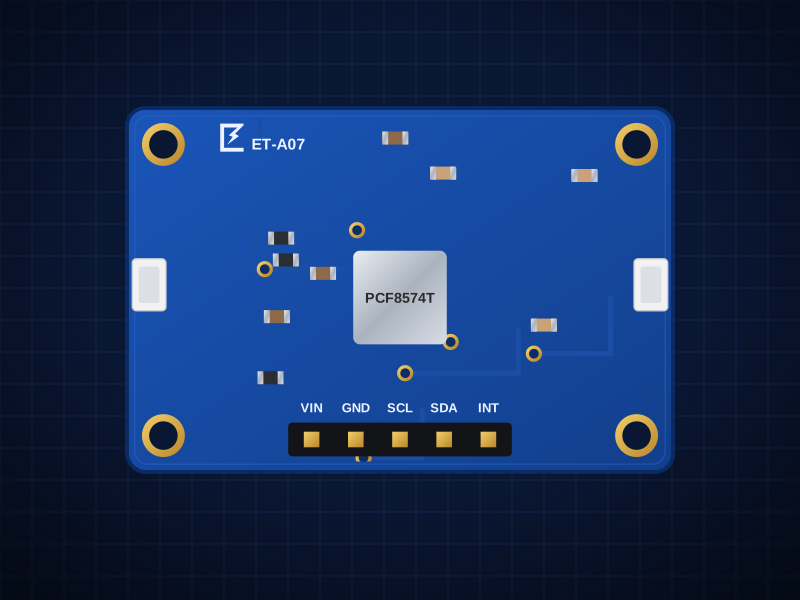
ET-A07
PCF8574 8-Bit I/O Expander
Eight extra GPIO pins over I²C, Qwiic
AED 14.00
Out of stockOverview
Eight extra GPIO pins over I²C, Qwiic
The ET-A07 is built around the NXP PCF8574T — 8 quasi-bidirectional I/Os, 25mA sink per pin (LEDs to VIN), interrupt output. It connects over I²C 100kHz (0x20 (0x20–0x27 via jumpers); Qwiic / STEMMA QT) and is powered from 2.5–6V.
Two Qwiic / STEMMA QT connectors let you chain it with other boards without soldering, and the 2.54 mm header fits a breadboard.
Designed in Dubai by ElectroTrical — the full schematic, BOM and design notes are published below.
Good for
- A few extra buttons or LEDs
- Driving relay boards
- Simple I/O on small boards
Key features
What makes it different
Expander
NXP PCF8574T: 8 quasi-bidirectional I/Os, 25mA sink per pin (LEDs to VIN), interrupt output
Interface
I²C 100kHz, 0x20 (0x20–0x27 via jumpers); Qwiic / STEMMA QT
Supply
2.5–6V
Libraries
PCF8574 (Rob Tillaart), Adafruit_PCF8574, CircuitPython adafruit_pcf8574
Qwiic / STEMMA QT
Two JST-SH connectors plus a 2.54 mm header — 3.3 V and 5 V hosts.
Open documentation
Schematic, BOM and layout notes published for every board.
Specifications
Technical specifications
| Expander | NXP PCF8574T: 8 quasi-bidirectional I/Os, 25mA sink per pin (LEDs to VIN), interrupt output |
|---|---|
| Interface | I²C 100kHz, 0x20 (0x20–0x27 via jumpers); Qwiic / STEMMA QT |
| Supply | 2.5–6V |
| Size | 38.1 × 25.4 mm |
|---|---|
| Mounting | 4 × M2.5 holes, 2.54 mm from each corner |
| Connectors | 2 × Qwiic / STEMMA QT (JST SH 4-pin) · 5-pin 2.54 mm header |
| Main IC | PCF8574T/3,518 (LCSC C7605) |
| Revision | Rev A |
| Libraries | PCF8574 (Rob Tillaart), Adafruit_PCF8574, CircuitPython adafruit_pcf8574 |
|---|
| JP1 (default Closed) | Power LED (cut = off) |
|---|---|
| JP2 (default Closed) | I²C pull-ups (cut = off) |
| JP3–JP5 (default Open) | Bridge to set A0–A2 → address 0x20–0x27 |
Performance
Scale
Pinout
Pin map and connections
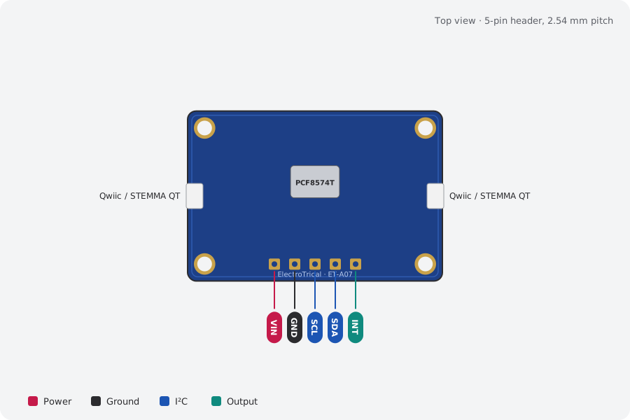
| Pin | Name | Type | Function |
|---|---|---|---|
| 1 | VIN | Power | 3.3–5V |
| 2 | GND | Ground | Ground |
| 3 | SCL | I²C | I²C clock |
| 4 | SDA | I²C | I²C data |
| 5 | INT | Output | Low = input changed |
Qwiic / STEMMA QT pins: GND, VIN, SDA, SCL (same on both connectors). I²C pull-ups (10 kΩ) are on the board; cut JP2 to remove them.
Mechanical
Dimensions and what's in the box
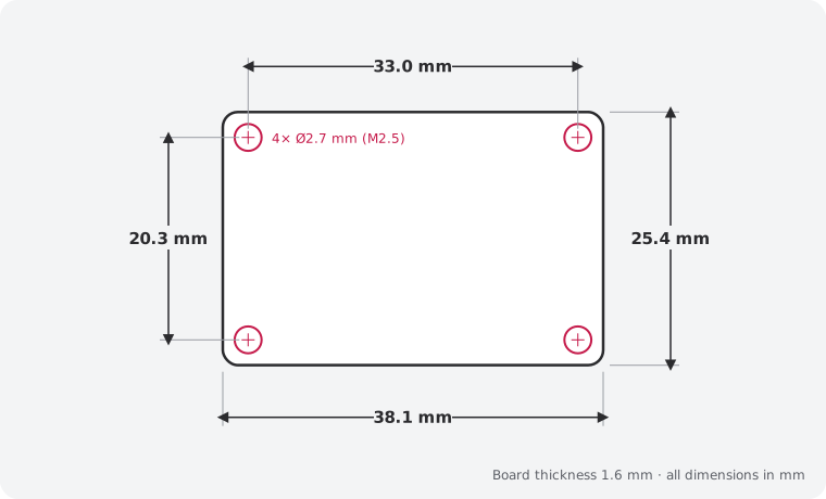
In the box
- 1 × ET-A07 PCF8574 8-Bit I/O Expander (assembled)
- 1 × 5-pin 2.54 mm male header, unsoldered
Getting started
- Plug in a Qwiic / STEMMA QT cable, or solder the header and wire VIN, GND, SDA and SCL
- Libraries: PCF8574 (Rob Tillaart), Adafruit_PCF8574, CircuitPython adafruit_pcf8574
- Run an I²C scanner to confirm the address: 0x20, 0x20, 0x27
Compare
Which I/O expander?
| PCF8574 8-Bit I/O Expander (this board)This board | ET-A04 MCP23017 16-Bit I/O Expander | ET-A03 4-Channel Level Converter | |
|---|---|---|---|
| What it does | Eight extra GPIO pins over I²C, Qwiic | Sixteen extra GPIO pins over I²C, Qwiic | Bidirectional 1.8–3.3 V ⇄ 3.3–5 V on four lines |
| Interface | I²C 100kHz, 0x20 (0x20–0x27 via jumpers); Qwiic /… | I²C up to 1.7MHz, 0x20 (0x20–0x27 via jumpers →… | — |
| Best for | A few extra buttons or LEDs | Button panels and keypads | 5 V sensors on 3.3 V boards |
| Price | 14 AED | 19 AED | 12 AED |
Downloads
Documents and design files
Need a custom version of this board?
Different connector, size or sensor? We design and build custom variants.